US 6,499,215 B1
Processing of circuit boards with protective, adhesive-less covers on area array bonding sites
Mark Kenneth Hoffmeyer,
Rochester, Minn. (US);
and Daniel Scott Johnson,
Rochester, Minn. (US)
Assigned to International Business Machines Corporation,
Armonk, N.Y. (US)
Filed on 29-Jun-2000, as Appl. No. International Business Machines Corporation,
Armonk, N.Y. (US)
Int. Cl.7H05K 3/34
U.S. Cl. 29-840
24 Claims
US 6,499,215 B1
Processing of circuit boards with protective, adhesive-less covers on area array bonding sites
Mark Kenneth Hoffmeyer,
Rochester, Minn. (US);
and Daniel Scott Johnson,
Rochester, Minn. (US)
Assigned to International Business Machines Corporation,
Armonk, N.Y. (US)
Filed on Jun. 29, 2000, as Appl. No. 9/606,583.
Int. Cl.7H05K 3/34
U.S. Cl. 298212;840
24 Claims
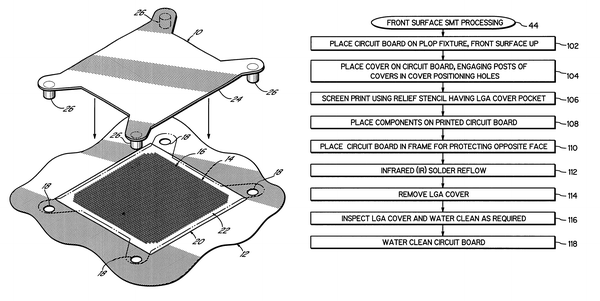
1. A method for processing a circuit board, the circuit board including an exposed area array bonding site, the method comprising:
overlaying a protective cover over the bonding site by registering a plurality of posts secured to one of the protective cover
and the circuit board into a plurality of apertures disposed in the other of the protective cover and the circuit board;
performing a fabrication process on the circuit board while the protective cover is overlaid on the circuit board wherein
the protective cover protects the bonding site from contamination associated with the fabrication, and
removing the protective cover.