US 6,499,217 B1
Method of manufacturing three-dimensional printed wiring board
Shingetsu Yamada,
Tokyo (Japan);
Jun Takagi,
Tokyo (Japan);
Koichiro Taniguchi,
Tokyo (Japan);
Kaoru Nomoto,
Aichi (Japan);
Toshihiro Miyake,
Aichi (Japan);
Kazuya Sanada,
Aichi (Japan);
and Makoto Totani,
Aichi (Japan)
Assigned to Mitsubishi Plastics Inc.,
Tokyo (Japan);
and Denso Corporation,
Aichi (Japan)
Filed on 24-Sep-1999, as Appl. No. Mitsubishi Plastics Inc.,
Tokyo (Japan);
and Denso Corporation,
Aichi (Japan)
Int. Cl.7H01K 3/22
US 6,499,217 B1
Method of manufacturing three-dimensional printed wiring board
Shingetsu Yamada,
Tokyo (Japan);
Jun Takagi,
Tokyo (Japan);
Koichiro Taniguchi,
Tokyo (Japan);
Kaoru Nomoto,
Aichi (Japan);
Toshihiro Miyake,
Aichi (Japan);
Kazuya Sanada,
Aichi (Japan);
and Makoto Totani,
Aichi (Japan)
Assigned to Mitsubishi Plastics Inc.,
Tokyo (Japan);
and Denso Corporation,
Aichi (Japan)
Appl. No. 9/700,992PCT Filed Mar. 24, 2000, PCT No. PCT/JP00/01841PCT Pub. No. WO00/59274, PCT Pub. Date Oct. 05, 2000.
Claims priority of application No. 11-084278 (JP), filed on Mar. 26, 1999.
Int. Cl.7H01K 3/22
U.S. Cl. 298212;848
6 Claims
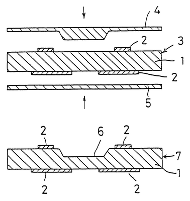
1. A method of manufacturing a three-dimensional printed wiring board, said method comprising the steps of providing a filmy
insulator comprising a thermoplastic resin composition containing 65-35 wt % of a polyaryl ketone resin having a crystal-melting
peak temperature of 260° C. or over, and 35-65 wt % of an amorphous polyetherimide resin, and having a glass transition temperature
as measured when the temperature is increased for differential scanning calorie measurement of 150-230° C., superposing a
conductor foil on one or both sides of said filmy insulator, heat-fusing said conductor foil so that said thermoplastic resin
composition will satisfy the relation between the crystal-melting calorie 916; Hm and the crystallizing calorie 916; Hc as expressed
((916;Hm8722;916;Hc)/916;Hm)8806;0.5, etching said conductor foil to form a conductor circuit, and deforming the printed wiring circuit obtained
three-dimensionally.